Genre: eLearning | MP4 | Video: h264, 1280×720 | Audio: aac, 44100 Hz
Language: English | VTT | Size: 4.02 GB | Duration: 14h 2m
What you’ll learn
We will cover the VHDL language and syntax with lots of examples
Relate VHDL code to hardware implementation
Creating FPGA building blocks using VHDL
Creating State Machines using VHDL
Creating complex FPGA designs from scratch
Highlight good design practice & common pitfalls
Writing Test Benches in VHDL
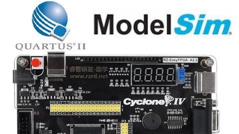
Simulate & debug FPGA Designs using ModelSim
Use the Intel Quartus software to compile and implement projects
Programming FPGAs using the USB Blaster
Implement a UART + State Machine project on a Cyclone IV FPGA
Requirements
Fundamentals of digital electronics & logic gates
Knowledge of binary and hexadecimal number systems
Description
This course is aimed at students & engineers who want to get into the field of FPGA development using VHDL.
We will start by covering the basics of FPGA hardware. This hardware background is vital and as we learn how to write VHDL, we will also refer back to how our code gets implemented in hardware.
In the second section of the course, we will cover the VHDL language in detail. We will cover all the aspects (Signals & Data types, VHDL Keywords & Operators, Concurrent & Sequential statements, Entity & Architecture, Process Block, Generics, Constants & Variables, Records, Component Instantiation, Procedures & Functions, Packages & Libraries and Type Conversions) that are needed to be able to develop complex and advanced FPGA designs. There will be plenty of simple examples to allow you to learn the VHDL language quickly and enable you to confidently write your own code. We will also look at how most of the VHDL language maps to hardware on the actual device.
With this strong foundation in the language, we will look at how to build fundamental FPGA blocks starting from Tri-State Drivers, Registers, Comparators, Multiplexers, Shift Registers, Serialisers, RAMs & ROMs and Finite State Machines. We will look at how to code all of the above structures and also explore how these are implemented in real hardware in the FPGA.
In the next section, we will look at hierarchical design with VHDL. This design practise is used when creating complex designs having more than one design unit. We will explore this concept from an example to see how design units can be joined together to form a hierarchical design.
In the next section we will explore good FPGA design practise. From my experience most beginners in FPGA design make common mistakes and fall into certain traps. Some of these can lead to issues that are very difficult to debug and fix. The idea behind this section is to make you aware of these common pitfalls and explore ways in which we can circumvent these. We will talk about Latches, Generated Clocks, Clock & Data Gating, Benefits of a Register Rich Design, Benefits of Synchronous Design, Dealing With Asynchronous Inputs, Clock Domain Crossing, Designing for Reuse, Signal Initialisation, Synchronising Reset De-assertion, Routing Clocks & Resets and Using PLLs.
At this point you should have the knowledge to create your own FPGA design using VHDL. We will now cover design verification. This section will explore how to write test benches. We will explore aspects of VHDL coding styles for writing test benches. We will discuss how to perform file IO for creating input vectors and to store output results. We will also discuss self-checking test benches to help automate the test process.
In the final section of the course, we will design a UART module controlled by a State machine. We will write VHDL code to implement the UART and state machine from scratch. We will use a hierarchical design approach where we will have a number of design units. We will write test benches for each design unit and perform simulations (using ModelSim) for verification. We will bring all design units together into our top level VHDL module and do a system level simulation. Next, we will explore how to create & configure a project in Intel Quartus to implement our design on our FPGA development board. We will look at how to do the pin assignments and also very briefly look at applying very basic timing constraints to get our design to pass. We will then test the design on real hardware to make sure our design works as intended.
Who this course is for:
Graduate students looking for a career as an RTL engineer or Design Engineer
Electronics engineers/hobbyists who want to get into the field of FPGA design
Those interested in FPGA development who are looking for an introductory course
Anyone about to embark on their first VHDL design project
Password/解压密码0daydown
Download rapidgator
https://rg.to/file/8c3d48d3123db17419c005e424999d02/Learn_FPGA_Design_With_VHDL_(IntelAltera).part1.rar.html
https://rg.to/file/6e2050fdd4fccdac6ca58b569cde918e/Learn_FPGA_Design_With_VHDL_(IntelAltera).part2.rar.html
https://rg.to/file/ef8849ac9e4ddc603bbbb6d78c7323aa/Learn_FPGA_Design_With_VHDL_(IntelAltera).part3.rar.html
https://rg.to/file/4930632b90735d4bc540b1995c956251/Learn_FPGA_Design_With_VHDL_(IntelAltera).part4.rar.html
https://rg.to/file/51ad6a75e2a72505df4663c12abb994d/Learn_FPGA_Design_With_VHDL_(IntelAltera).part5.rar.html
Download nitroflare
https://nitroflare.com/view/56566C62B134084/Learn_FPGA_Design_With_VHDL_%28IntelAltera%29.part1.rar
https://nitroflare.com/view/5F9F771FA8ABFC2/Learn_FPGA_Design_With_VHDL_%28IntelAltera%29.part2.rar
https://nitroflare.com/view/B739D0C7360451C/Learn_FPGA_Design_With_VHDL_%28IntelAltera%29.part3.rar
https://nitroflare.com/view/28F6792C5ABA08E/Learn_FPGA_Design_With_VHDL_%28IntelAltera%29.part4.rar
https://nitroflare.com/view/ECAE5AD4ACD5ED3/Learn_FPGA_Design_With_VHDL_%28IntelAltera%29.part5.rar