MP4 | Video: h264, 1280×720 | Audio: AAC, 44.1 KHz, 2 Ch
Genre: eLearning | Language: English + srt | Duration: 16 lectures (3h 48m) | Size: 1.65 GB
Learn PCB design and Electronic circuit analysis with PADS Pro (license is included)
Learn PCB design and Electronic circuit analysis with PADS Pro (license is included)
What you’ll learn:
Students will learn PCB Design with one of the most in demand software tools PADS Professional
Students will learn and get to practice with modern circuit electronic analysis techniques through simulation
Access to PADS Standard edition license for 1 year
Students will get the chance to recreate multiple circuit designs in PADS professional
Students will learn to hone their skills in design and development, specially those needed for interviews
Get access to the like minded professional community where students and professionals get to work with each other
Students will learn working with CAD files in PADS software and build their own PCB layout and routing
Requirements
Willing to learn and dedicate time to practice
Basic understanding of the circuit (OHM Law) and Electronic components (Resistor, Capacitor, etc)
A capable Windows PC or a virtual machine for running PADS Professional and working with CAD files
Pads pro Designer VX.2.6 or VX.2.7 ( License will be provided in this course)
Description
Learn PCB design with Pads Professional, Siemens’s circuit design software (Software License is included)
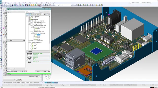
One of the key parts of electronic design is creating a printed circuit board (PCB) but there are many challenges that many engineers face within a complex PCB design. Pads Professional is a powerful integrated circuit design software that supports a variety of PCB design needs and provides affordable features to help engineers to get products to market faster.
Pads layout software offers sketch routing tool that is an automated intelligent routing method to speed up PCB design and, hence, it reduces the PCB design time dramatically. In this software, the remarkable routing of automation capabilities are:
fan-out for signals, hierarchical 2D/3D planning & placement, dynamic copper pour, dynamic planes, tuning of high-speed nets, and sketch routing.
Hyperlynx thermal analysis is the other capability provided by this software that allows engineers to analyze the effect of heat generated by components and meet the thermal constraints
Integration between schematic and layout workspace is the other helpful feature that reduces errors within designing
A large number of parts, symbols, and footprints are accessible on the PARTQUEST website and you can download and use them in Pads Professional software, so it can be the other advantage of PADS-designed software.
In this course, we will focus on essential tools and features in pads professional software to create printed circuit boards and you will learn what you need to know about designing your own PCB by using this software.
The summary of each section’s content is as below:
Introduction to the interface
Creating a new project
Using navigator panel
Introducing useful windows and panels
How to define the border size
PARTQUEST
How to use the PARTQUEST website to find the desired parts, symbols, and footprints
How to add each part into the pads pro designer workspace
How to categorize a special group of components to access them quickly
Placing and wiring parts
Using search window and my parts panel to access required components and place them in the schematic workspace
How to manipulate the placed components
Using a net tool to wire the components
Creating a circuit diagram as an instance and utilize the mentioned tools
Using DRC or how to use verify tool to find the design rule violations
How to specify design rules or physical characteristics to set the constraints by using constraint manager
Creating a PCB file
Mapping components in the logical pads designed to the physical footprint
How to work with component explorer
How to place the components by using schematic workspace to reduce the errors within designing
Creating a group of components that is helpful in a large, dense design
How to edit the placed components
Defining the physical borders of PCB
Routing the PCB
Introducing DRC in pads layout environment
How to work with net explorer and cross probe to facilitate routing
How to work with a fan-out tool to add Vias
Showing different methods of routing and how to work with them
How to add Vias and change the layers
How to find unconnected net lines
Defining plane layers and nets to have more uniform connectivity, decrease impedance and reduce complex routing
How to have a 3D view of PCB board
Synchronizing the 2D and 3D views simultaneously
Adding dimension to PCB board
Manufacturing output
How to generate output file
Adding netlabel and bus
Connecting nets by using netlabel to speed up the process of schematic designing and reduce mistakes
How to represent multi-wire connections by using Bus tool
Sketch route
Automating routing by using sketch route capability
Tuning
How to create tracks with the same length in high-speed connections
Creating new symbols and cell
How to work with Symbol Editor and create a new symbol
How to create Package Cell
How to specify the new cell for created symbol
Hyperlynx thermal
Simulation of Thermal Impact of PCB placement and routing
How to work with Hyperlynx thermal tool to analyze the effect of the heat generated by the components
Projects
In this project, you will learn how to build a temperature sensor circuit using Pads Professional
What you will learn
Learn circuit design and PCB design by using the most powerful integrated circuit design software, Pads professional
Use verify tool to find the design rule violations
Learn essential methods to automate routing and speed up routing process
Defining plane layers
Creating desired symbols and footprint based on your need
Hyperlynx thermal analysis to simulate the thermal impact of PCB
Defining the physical borders of PCB
Who this course is for
Students who are interested in learning PCB design and circuit analysis
professionals who want to learn PADS Professional for building modern PCB circuit
Electrical & Electronic engineers
PCB Layout Designers
Anyone interested in circuit designing and creating printed circuit board
Researchers
Download rapidgator
https://rapidgator.net/file/890c94429cde315c716edc1db71674b1/0817_21.z01.html
https://rapidgator.net/file/88c5c33e46ba5840b72476bd997efa11/0817_21.zip.html
Download nitroflare
https://nitro.download/view/2805382C44CCABC/0817_21.z01
https://nitro.download/view/5DD9CC23C108457/0817_21.zip
